
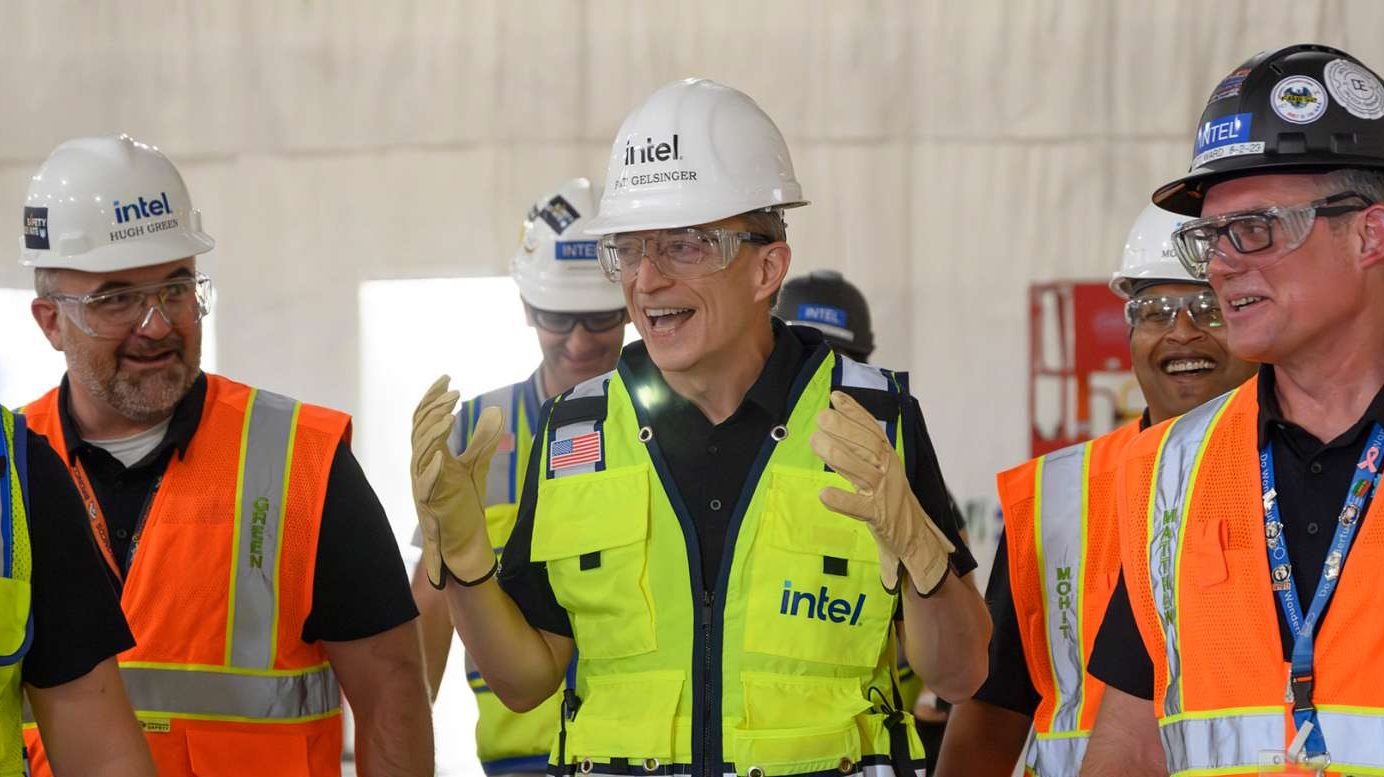
The machine weighs 165 tons and cost around $400 million, and Intel has put it to work. On July 15, ASML confirmed that Intel Foundry has become the first chipmaker anywhere to ship high-volume logic chips made with High-NA EUV lithography, the next generation of the extreme ultraviolet technology used to pattern the world’s most advanced processors. The chips are part of Intel’s Core Ultra Series 3 laptop processors, codenamed Panther Lake, built on the company’s 18A manufacturing process.
The announcement closed a chapter that began with skepticism. High-NA EUV, which raises the numerical aperture of the light path from 0.33 to 0.55, lets chipmakers print features as small as roughly 8 nanometers, smaller than the 13.5-nanometer limit of the previous generation of machines. The technology was considered years away from production when ASML delivered its first High-NA scanner to Intel’s D1X fab in Hillsboro, Oregon, in 2024. Intel was the first and, for a long time, the only customer willing to bet on it.
The Oregon facility is where the bet is paying off. Intel is using High-NA to pattern a subset of layers on Panther Lake, and the company said yields on those layers already match its mature EUV tools. The layers are dual-qualified, meaning they can also be produced on conventional EUV machines, a hedge that lets Intel keep production running while it learns the new technology. The result, according to people familiar with the operation, is that Intel has dialed in the process without betting the node on it.
The strategy is deliberate. The 18A process was designed around low-NA EUV and multi-patterning, and it does not depend on High-NA to ship. By threading High-NA into a node that would be fine without it, Intel gives its engineers practice with the machine before it becomes a necessity on the 14A and 10A nodes that follow. The company learned the cost of caution in the 10-nanometer era, when its delay in adopting EUV cost it years of leadership; this time it is adopting the next machine early.
The news arrived with a second shift in Intel’s manufacturing plans. Intel is reducing its outsourced orders for Nova Lake, its next-generation desktop and mobile processor line, moving more of the production to its own 18A process instead of paying Taiwan Semiconductor Manufacturing Co. for 2-nanometer wafers, according to reports this week. The change is a vote of confidence in Intel’s own process technology and a sign that management believes its fabs can handle the company’s most important products.
The manufacturing turnaround has been the centerpiece of Intel’s strategy since Pat Gelsinger launched the IDM 2.0 plan, and the strategy has outlived its architect. After Gelsinger’s departure, the company’s new leadership, under chief executive Lip-Bu Tan, has continued the foundry push while pressing for results. Tan has said monthly yield gains on 18A are running 7% to 8%, and the High-NA announcement gives him a concrete achievement to point to.
The financial stakes are clear in the company’s own statements. Chief financial officer David Zinsner has told investors that signals from prospective foundry customers should become “more concrete” in the second half of 2026 and into early 2027. Microsoft and Amazon Web Services have been named as companies evaluating Intel’s advanced nodes, though no commitments of the scale that would move Intel’s financials have been announced.
The hard part is converting manufacturing capability into revenue. Intel’s foundry business has yet to sign the kind of anchor customers that would fill its fabs, and the customers Intel wants most, the AI chip designers who currently build with TSMC, have shown no signs of switching. Lithography leadership and foundry revenue are different things, and the High-NA achievement does nothing for the balance sheet unless outside customers sign wafer agreements.
The competitive context is unforgiving. TSMC’s customers stayed with it through a decade of Intel’s stumbles, from repeated 10-nanometer delays to the scrapped 20A node, and trust of that kind does not rebuild on the strength of one scanner hitting its yield target. Intel’s pitch to prospective customers now rests on a new technology, a new leadership team and a promise that the execution problems of the past are fixed.
For ASML, the Intel announcement is validation of a different kind. The Dutch company has spent years selling High-NA as the industry’s next tool, and Intel’s willingness to use it in volume production is the evidence ASML needs to convince other chipmakers that the machine is real. ASML has said the technology is in a validation phase; Intel’s shipment moves it into commercial use.
The products themselves are already in the market. Panther Lake, introduced at CES in January and on sale since late January, is Intel’s mainstream laptop chip, and the High-NA-produced units are a portion of that line. The company’s Wildcat Lake processors and Arc G3 handheld products followed in the spring. Each generation gives Intel more High-NA data and more reason to scale the technology.
The long-term picture is what the company is really selling. Intel has said 14A will build High-NA in as a requirement rather than an option, and the lessons learned in Oregon will shape chips that do not ship for years. Whether that arc leads Intel back to leadership or merely keeps it in the race will be decided by the customers it can sign in the meantime. For one day, at least, the machine at D1X did exactly what it was supposed to do.