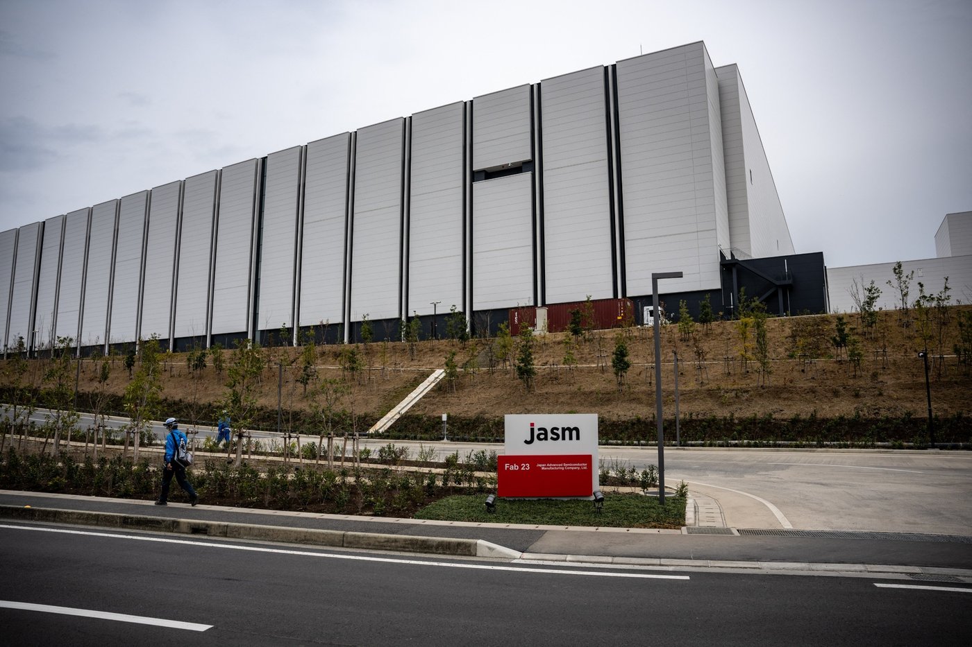

TOKYO–Kumamoto prefecture, on the southern island of Kyushu, has become the most crowded patch of semiconductor real estate in Japan. TSMC’s first Japanese fab opened there, its second is under construction next door, and a steady stream of suppliers has followed. Now the region is getting a new neighbor with a different specialty: Sony, the world’s largest maker of image sensors, plans to build its next factory beside the Taiwanese chipmaker’s campus.
The two companies are investing roughly 1 trillion yen, about $6.3 billion, in a new plant in Kumamoto to make advanced image sensors, with mass production targeted for 2029, according to Nikkei, which first reported the plan. Sony will operate the facility, which will manufacture the sensors that go into smartphone cameras, and TSMC will provide the advanced processing capacity to make them.
The project deepens a partnership that has been quietly expanding for years. Sony and TSMC began collaborating on image sensor production in 2021, when Sony outsourced some logic processing to the Taiwanese company’s fabs. The new plant, located next to TSMC’s Kumamoto campus, is designed to capture the supply-chain efficiencies of co-location: sensors move from fabrication to packaging without leaving the region.
The investment targets a specific demand: the camera upgrades coming to Apple’s iPhone lineup and the growth of machine vision in robotics and autonomous systems, a market Sony executives have described as “physical AI.” Image sensors are the eyes of that world, and Sony, which supplies the cameras in most high-end smartphones, is positioning itself to serve it at scale.
Sony’s dominance in image sensors is rarely challenged. The company holds roughly half of the global CMOS sensor market, supplying Apple, Samsung, and most other phone makers. But the technology is demanding: advanced sensors require logic chips fabricated on leading-edge processes, which Sony historically did not own. The partnership with TSMC solves that problem by pairing Sony’s sensor design with TSMC’s manufacturing.
The new plant’s economics depend on smartphone volumes, which have plateaued globally, and on the success of physical AI, which remains an emerging category. Analysts said the 2029 production target gives Sony time to see which market materializes, and that the co-location with TSMC keeps costs competitive against rivals such as Samsung and a growing group of Chinese sensor makers.
The project also fits Japan’s industrial policy. Tokyo has designated semiconductors a priority sector and has funded TSMC’s Kumamoto expansion with subsidies, viewing the island’s chip cluster as a hedge against supply-chain concentration in Taiwan. Sony’s plant extends that logic: another advanced semiconductor facility, owned by a Japanese company, producing in Japan.
For TSMC, the deal is a win on two fronts. It secures a major customer for its Japanese capacity, helping fill the fabs it is building in Kumamoto, and it deepens the company’s relationship with Sony, one of the few Japanese companies that designs chips at global scale. The arrangement mirrors TSMC’s partnerships in the United States, where it manufactures for customers including Apple and Nvidia.
Construction timelines are already taking shape. The site preparation near TSMC’s Kumamoto campus has begun, according to people familiar with the plans, and both companies have signaled they will seek Japanese government support for the project. Subsidies, which covered roughly half the cost of TSMC’s first Kumamoto fab, are expected to play a similar role here.
The plant will also test Japan’s ability to build out its chip workforce. The region has absorbed thousands of TSMC employees and suppliers in four years, straining local infrastructure and labor markets. Sony’s plant will add more demand for engineers, and both companies have been recruiting across Kyushu and beyond, according to people familiar with the hiring efforts.
Sony’s sensor business has been a reliable profit engine, and the company has said it will keep investing in it even as its gaming and entertainment divisions grow. The company’s sensor unit posted steady margins through the smartphone downturn, and executives have pointed to automotive and industrial imaging as the next growth wave.
The physical AI narrative has attracted broader attention in Japan’s technology industry. The term, popularized by Nvidia’s Jensen Huang, describes machines that perceive and act in the physical world, and it implies enormous demand for the sensors, chips, and software that make it work. Sony’s bet is that Kumamoto, with its cluster of fabrication, will be where a meaningful share of that hardware gets made.
Risks remain. Smartphone camera upgrades are incremental, and the premium Sony charges for its sensors could face pressure from lower-cost competitors. The physical AI market could grow more slowly than the industry’s most optimistic projections. And the 1 trillion yen investment, split with TSMC, must ultimately be paid for by product revenue starting in 2029.
The companies are betting on the long game. Sony’s position in imaging has survived every technological shift of the past two decades, from digital cameras to smartphones, and TSMC has become the indispensable factory floor of the semiconductor industry. In Kumamoto, the two are building the infrastructure for the next decade of both businesses, one wafer at a time.