
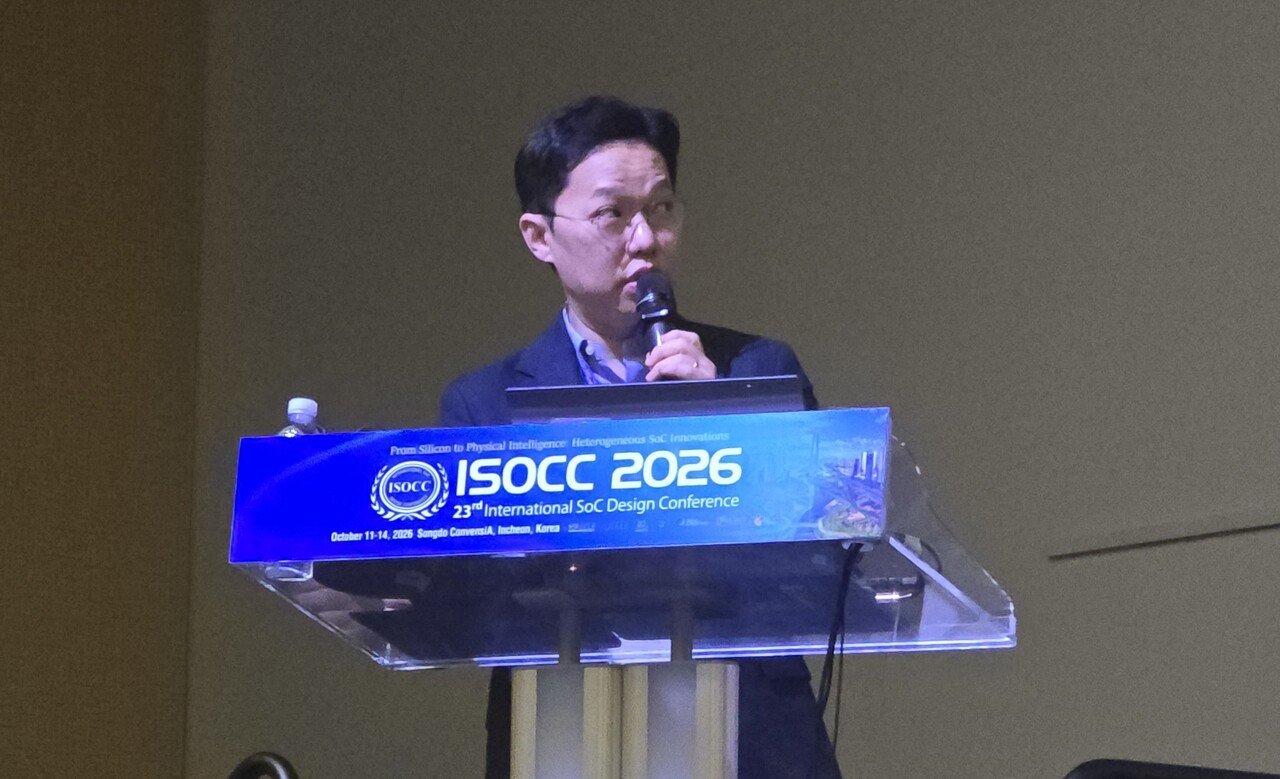
SK Hynix disclosed the design of a small processor built for solid-state drives on October 12, and the architecture behind it breaks with the way controllers have been built for twenty years.
The chip is called the Hynix Transaction Processing Unit, or H-TPU. Instead of concentrating the drive’s housekeeping in one general-purpose CPU core, SK Hynix distributes that work across roughly 100 tiny programmable units on the controller die, each handling a narrow slice of the input and output traffic. Koo In-je, the vice president who runs SoC design at the company, presented the structure at the International SoC Design Conference in Incheon.
“The general-purpose CPU inside SSD controllers has reached its limits in power consumption and area,” Koo said, according to the company’s account of the event. SK Hynix developed the H-TPU to take over the common I/O path, he said, so the processor can do the repetitive work efficiently.
The numbers the company published are striking. Per core, an H-TPU uses 2.5% of the power of a general-purpose CPU core and about 4% of its silicon area, Koo said. Those units run a four-stage pipeline with sequential execution, a design chosen for jobs that repeat rather than jobs that branch. When a specific request arrives, only the units needed for it wake up; the rest stay idle.
What remains with the general CPU is the irregular work: recovering from errors, handling exceptions, managing storage policy. That division of labor is the same logic that put graphics work on GPUs and matrix arithmetic on NPUs. Repetition belongs on small, cheap, specialized cores, and control flow belongs on the one core that has to be flexible.
The pressure forcing the change is familiar to anyone who has watched NAND evolve. Each generation of flash reads and writes faster than the last, and each increase adds work inside the controller: more outstanding commands, more metadata to track, more buffer juggling. The standard response was to add CPU cores, usually licensed from Arm, which are engineered for complex computation and are therefore an expensive way to process a stream of similar instructions. Controller power and area grew with every generation, and in a dense enterprise rack neither is cheap.
SK Hynix says it built development tools as well, including a dedicated compiler, so that engineers can write code for the array of small units without rewriting it for each one. Whether outsiders adopt that toolchain will decide whether the H-TPU stays an internal design or becomes a platform other drive makers can build on.
The company has a roadmap for it. H-TPU units are headed into next-generation enterprise SSD controllers and, eventually, across several NAND product lines. The technology also feeds an architecture SK Hynix calls Storage Next, aimed at a specific habit of AI models: reading data in chunks smaller than 512 bytes, one-eighth the 4-kilobyte size that NAND hardware hands out by default. The company has said it plans to put H-TPU into high-bandwidth flash, a product it expects to ship next year.
Storage Next is where the commercial argument sits. Enterprise flash has become one of the tighter links in AI infrastructure, because training runs and inference servers both pull small pieces of data from drives constantly, and each of those fetches costs the controller power and time. Drive capacity has stopped being the only thing customers ask about. Latency per read matters as much, and so does the wattage the drives add to a rack that already draws as much as a substation.
The market is paying for drives that answer quickly. Enterprise SSD orders tied to AI servers have pushed NAND prices higher through the year, and on October 13, the day after Koo’s presentation, S&P raised Kioxia Holdings’ long-term credit rating one notch to BBB with a positive outlook, citing enterprise SSD demand and the improvement in cash flow that came with it.
Competition in controllers runs along the same seam. Samsung and Micron build controllers in house for their own drives, while Marvell, Silicon Motion and Phison sell controller silicon to everyone else, and each has been pushing power efficiency as flash layers multiply. None of them has published an architecture that spreads command processing across a hundred small units, which is what makes the H-TPU disclosure worth reading.
Two cautions apply. The power and area figures come from SK Hynix, measured against its own baseline, and no independent lab has reproduced them. A 40-fold reduction in per-core power does not translate into a 40-fold reduction in controller power, because the general CPU was never the whole budget: the PHYs, the DRAM interface and the flash channels consume most of it. The savings will show up as headroom, not as a revolution.
The second caution is timing. Storage Next and high-bandwidth flash are plans, and memory roadmaps have a long history of slipping by a year or two. H-TPU into next-generation controllers is the near-term promise, and enterprise drives using it are the first place to check whether the architecture delivers outside a conference keynote.
What SK Hynix has done, though, is name a problem the industry had been absorbing quietly. Controllers were getting bigger, hotter and more expensive to design, because the CPU cores inside them were never meant for the job. If a hundred small processors can do that work at a fraction of the cost, the answer will show up in drive power figures within a generation or two, and every NAND maker will have to respond.
The company built its compiler before it needed outside customers, which is usually a sign a design is meant to last longer than one product cycle.