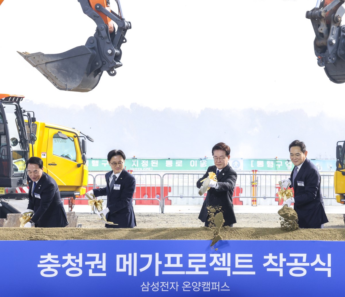
The Onyang complex outside Asan has assembled and tested conventional memory chips for four decades, through three downturns and two booms. On Thursday, a group of officials and executives stood on the site of a new line there with shovels.
Samsung Electronics held a groundbreaking ceremony at its Onyang campus in Asan, South Chungcheong Province, to convert the site into a hub for advanced packaging of high-bandwidth memory. President Lee Jae Myung and Samsung Chairman Lee Jae-yong attended. The project pairs a 6 trillion won packaging fab with 40 trillion won of phased equipment spending, roughly $34.5 billion in total, with production targeted for June 2028.
“Just four months later, we are standing at the site where that promise is becoming reality,” the president said, referring to an industrial plan his government announced in late June.
Samsung has moved construction up by about a year. The building will be three stories with roughly 31,000 square meters of cleanroom space, and it is designed to package HBM4E, the generation of memory that chipmakers expect to supply the accelerators shipping in 2028.
Packaging has moved from a back-end chore to a bottleneck. HBM is made by stacking layers of DRAM and connecting them with vertical pathways, and the yield of that stack decides how much usable memory comes out of a wafer. The bonding, the thermal interface and the testing all happen at plants like Onyang, and the equipment for those steps is in short supply.
That is where the money has gone. Memory makers have spent two years adding cleanroom space for the stacking step while their customers sign supply agreements years ahead. SK Hynix established a lead in HBM and has held it, which is the gap Samsung is trying to close with capacity rather than with a single product.
The ceremony had a second purpose that had little to do with memory. The project is the first of three industrial programs the government unveiled in late June, covering semiconductors, AI data centers and physical AI. In July, Samsung, SK Hynix and other companies pledged about 392 trillion won, or roughly $295 billion, of investment in the central Chungcheong region.
Speed is part of the political argument. The province and the city of Asan cut permitting to about a third of the usual time, and the president promised that the central government would help secure the electricity and water the plants need. Six of the eight companies in the Chungcheong program have begun spending, according to the government.
Pushing capacity south of Seoul is a longstanding goal. The capital region holds about half the country’s population and most of its skilled engineers, and successive governments have tried to move advanced manufacturing outward without much success. A plant that opens in 2028, with equipment arriving from next year onward, will test whether the permits stay fast once the cameras leave.
The commercial risk is the calendar. Memory has never been a business in which a plant built for demand four years out is guaranteed a market when it opens. The construction period spans at least two pricing cycles, and the HBM generation this plant is designed for will compete with whatever SK Hynix and Micron can make by then, at prices set by the least efficient producer.
There is a demand argument that did not exist in earlier cycles. HBM sells on contracts that stretch longer than conventional DRAM, and the buyers are a small group of accelerator designers whose road maps are public. If those road maps hold, the capacity has a home. If one of them slips a generation, the plant is left with equipment configured for a part nobody is buying.
Cost is the other variable. A packaging fab is cheaper to build than a wafer fab and slower to write off, which is why Samsung can commit to equipment before the memory price recovers. The 40 trillion won of tooling will be ordered in stages, and each stage can be deferred if the market turns, an option the ceremony did not mention but the budget implies.
Samsung’s own record cuts both ways. It has been the largest memory maker by volume for most of the past two decades, and it has also been the company that kept building through downturns and took share when rivals pulled back. That habit is expensive, and over a full cycle it has usually paid.
For the government, the plant is a test of a method: select a sector, gather the chaebol, shorten the permits and announce the result. For Samsung, it is a bet that the packaging step stays scarce long enough to justify the equipment order. Both are unanswered by a ceremony.
The question left open is whether the four-month sprint from announcement to shovel becomes a habit or remains a single exception. The next two projects in the program will show which.