Samsung Electronics bought two of the most advanced chipmaking tools ever built, then decided to let them wait. ChangMin Park, a senior technology executive at the Korean company, told engineers at a lithography conference in South Korea that ASML’s High-NA EUV scanners would not enter volume production until Samsung’s A10 node, a one-nanometer-class process scheduled for around 2030. The admission landed like a delay notice for the Dutch supplier’s priciest product line.
Samsung had earlier said it would put High-NA EUV to work at its two-nanometer and 1.4-nanometer nodes. Park now said the machines will become necessary only from A10 onward, according to people who attended the session. Until then, Samsung plans to keep using its existing 0.33 numerical aperture EUV tools with multi-patterning, the slower and more expensive workaround that prints the finest circuits by exposing the same layer several times.
The shift is part of a broader retreat in Samsung’s foundry roadmap. The company’s 1.4-nanometer process, once promised for 2027, has been pushed to 2029, leaving a longer gap between its two-nanometer products and the next shrink. That timeline puts the company roughly three years behind TSMC on leading-edge nodes, a gap that a decade of foundry investment has not yet closed.
The two High-NA machines Samsung already owns sit at its Hwaseong campus. The company installed the first last year and a second in the first half of 2026, a commitment of more than one trillion won, roughly $740 million, according to local reports. The tools are being used for development work, not for making chips that ship to customers. Bringing them into full production now would raise costs sharply at a moment when Samsung is trying to turn around a foundry business that has shed market share.
Price is the central reason for the caution. A single High-NA EUV scanner costs about $400 million, roughly twice as much as the low-NA machines already on factory floors. The technology also still needs work on masks and protective films, Park said, echoing a view that the equipment is not yet mature enough for high-volume manufacturing. Samsung appears to have decided that the yield and cost benefits of High-NA do not yet justify the expense before the one-nanometer node.
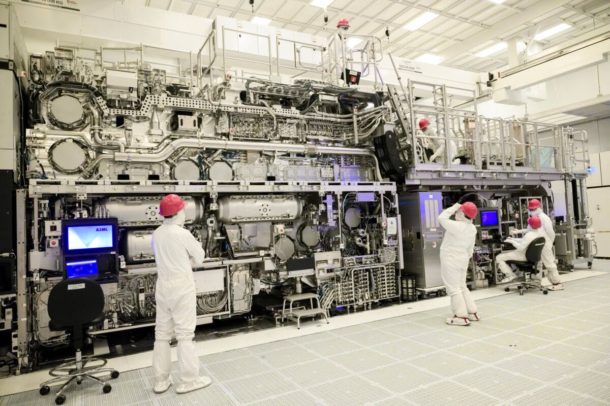
High-NA, short for high numerical aperture, is the tool ASML designed to keep Moore’s Law moving past the limits of its current machines. Where the standard scanners use a 0.33 numerical aperture lens, the new models use 0.55, gathering more of the light reflected off the mask to resolve smaller features in a single exposure. That single-pass capability is the product’s entire economic argument: it promises to replace multi-patterning, which can require three or four passes per layer, with one cleaner step.
TSMC reached a similar conclusion earlier. The Taiwanese foundry has bought High-NA systems strictly for research and has said it will not use them on its A13 or A12 nodes, which are expected to enter production around 2029. TSMC has signaled it will adopt the machines only once the benefit is, in its words, meaningful and measurable. The two largest chip foundries now share a position: the technology’s commercial moment is not this year and not next.
Intel is the outlier. It installed the first commercial High-NA system at its Oregon fab in April 2024 and has put the machines to work on its 18A process, the node behind its Panther Lake and Core Ultra Series 3 processors. Intel accepted higher near-term cost in exchange for a performance lead, a bet it could afford to make because it is fighting to regain ground rather than defend it.
Investors read Samsung’s timeline as a setback for ASML. The Dutch company is the only maker of High-NA scanners, and its order book has come to depend on customers committing to the technology. Shares of ASML fell as much as 3.3 percent in European trading on Oct. 1 after the remarks circulated, a sign of how sensitive the stock is to any hint that the industry’s migration to its newest tools is slipping.
The decision also exposes the arithmetic of the next generation of chips. High-NA’s appeal is that it prints smaller features in a single pass, cutting the number of exposures a chip needs. But as long as multi-patterning on existing tools can still reach the required dimensions, the case for spending $400 million a machine, and retraining fabs around it, is weaker than the marketing suggests. Samsung is betting it can afford to wait.
For ASML, the risk is a thinning of near-term demand for its flagship product. Intel remains a customer, and memory makers such as SK hynix are evaluating the tools for next-generation DRAM. But with the two largest foundries deferring volume adoption to 2030 or beyond, revenue the company once expected to arrive this decade may come late and in smaller batches. Samsung’s quiet conference-room admission reset the clock on the industry’s most expensive machines.