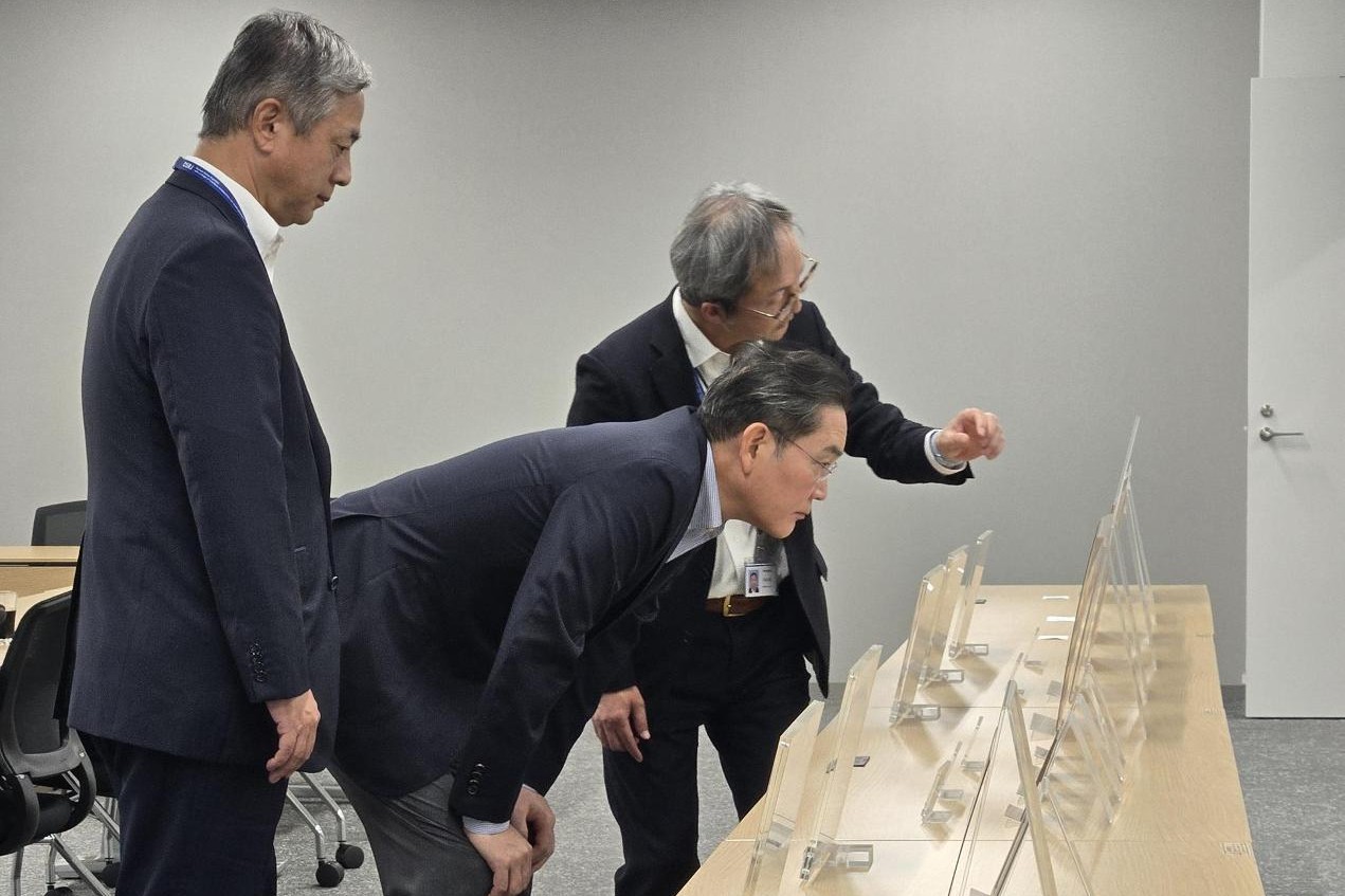
Lee Jae-yong flew to Japan this week to inspect a laboratory with a five-year budget of 350 billion won, about $262 million. Samsung Electronics spends several times that sum on equipment in a month. The chairman’s presence, announced by the company on Nov. 1, was the point: the small line item is attached to the step that has become the industry’s newest bottleneck.
The lab, called the Advanced Packaging Lab, sits inside Samsung’s research operations in Japan and is being positioned as a global hub for work on how chips are assembled after they leave the fab. Samsung said it will spend the 350 billion won, roughly 40 billion yen, over the five years through 2028.
Packaging used to be the part of the business nobody outside the industry discussed. A processor was made, put in a package, tested and shipped. The economics were thin and the technology was mature. That changed when AI accelerators began stacking high-bandwidth memory beside a logic die and connecting the pieces with thousands of microscopic wires. The assembly step now governs how fast data moves between the memory and the processor, which is close to governing how fast the processor is.
The result is a queue. Samsung’s smaller rival SK Hynix took the lead in high-bandwidth memory, the stacked DRAM that sits next to Nvidia’s accelerators, and has held most of that business through the current generation. Taiwan Semiconductor Manufacturing Co. controls the advanced packaging capacity that turns those memory stacks and logic dies into a working module, and its customers book that capacity years ahead.
Samsung has both a memory business and a foundry, which should make it the natural supplier of an integrated part. It has struggled to convert that position. Its high-bandwidth memory took longer than expected to clear qualification with the largest buyer of AI accelerators, and its foundry has won fewer large customers than its capital spending implied. The packaging lab is an attempt to fix the third leg of a three-legged stool.
Japan is a deliberate choice. The country supplies the materials and tools that packaging depends on: the temporary bonding adhesives, the grinders that thin a wafer to a hundredth of a millimeter, the inspection systems that find a crack before it becomes a recall. Japanese suppliers hold large shares in several of those categories, and several of them are small enough that a customer willing to co-develop gets engineering attention rather than a catalog.
The relationship has a history. In 2019, Japan restricted exports of three materials used in chipmaking to South Korea, and the dispute disrupted supply chains for both countries’ manufacturers before it was eased. Samsung kept its research presence in Japan through that period and has since expanded it. Lee’s own ties run back further: he took an MBA at Keio University in Tokyo, which gives the trip a personal history as well as a commercial one.
The visit also carries a message for Samsung’s domestic audience. Korea’s government has been pushing the country’s chipmakers to keep advanced work at home, and a chairman who travels to inspect a foreign lab is making a case that the work in question cannot be done anywhere else as well. The company framed the trip as a review of a global research hub rather than a shift of production, and no manufacturing capacity is moving.
The technical work at the lab is likely to concentrate on two methods. The first is hybrid bonding, which joins two wafers or dies with copper pads pressed directly together instead of solder bumps, cutting the distance a signal travels and the power it burns. The second is panel-level packaging, in which chips are assembled on large rectangular substrates rather than round silicon wafers, a change that lowers cost per unit if the yield holds. Both are manufacturing problems as much as design problems, and both reward the supplier who owns the materials.
For the industry, the more consequential question is whether packaging capacity becomes the constraint that decides who can sell AI chips at all. The memory makers can build stacks. The foundries can build interposers. The companies that can do both, at volume and at a yield that holds, are few. Samsung is trying to be one of them with a budget that is small against its capital spending and large against what a lab usually receives.
The five-year figure works out to 70 billion won a year. Samsung’s capital spending on facilities has run above 40 trillion won in recent years. The gap describes what the company believes the lab is for: not capacity, but know-how it can carry back to factories in Korea, where the actual packaging lines are being built.
The program runs to 2028, by which point the memory stacks in the largest AI systems will have gone through at least two more generations, and the assembly step will have been asked to solve a problem nobody has specified yet.