
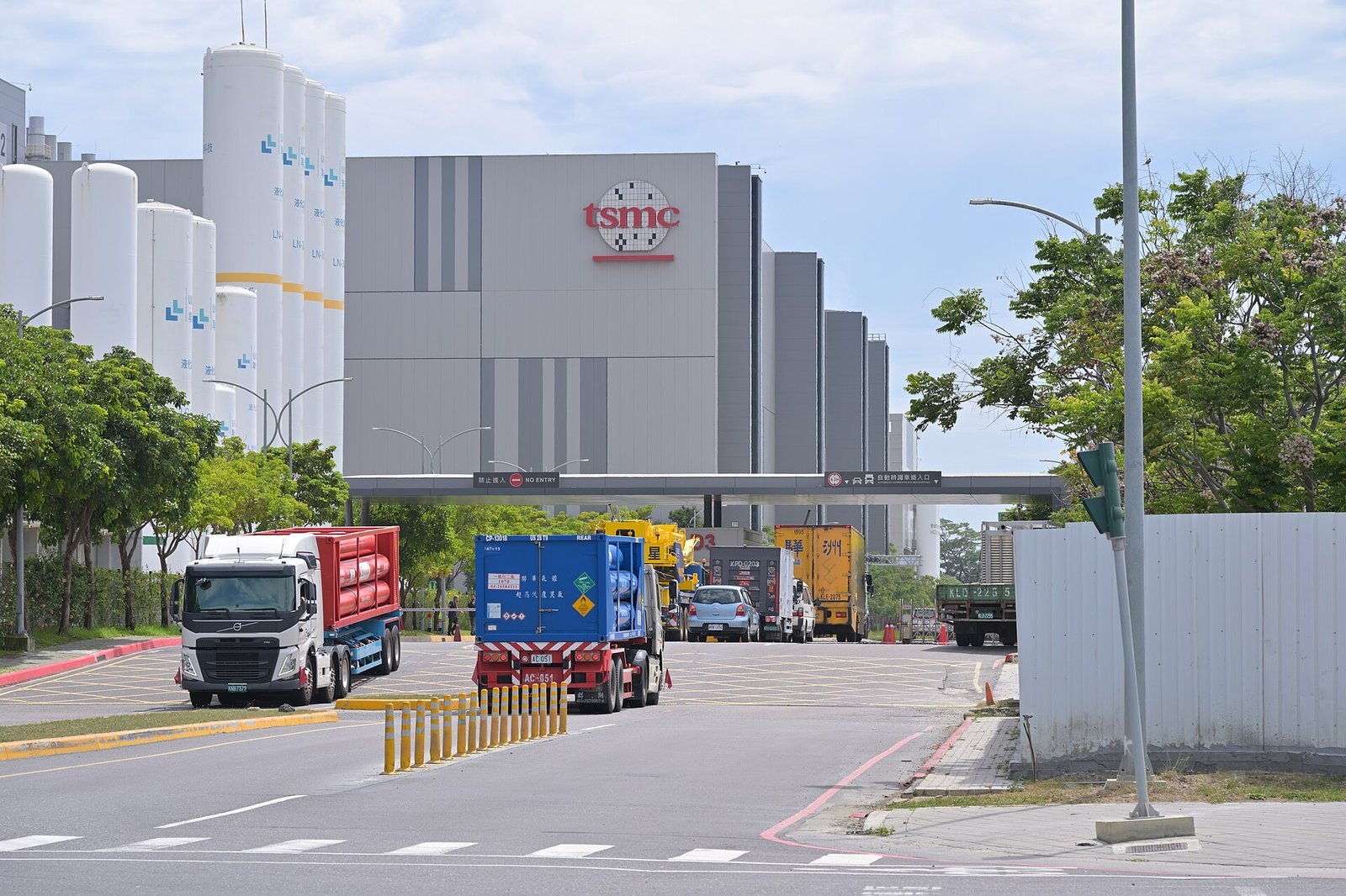
For eight years the least movable number in leading-edge chipmaking has been the size of a memory cell. Since the N5 process began volume production in 2020, TSMC’s high-density 6T SRAM bit cell has held at roughly 0.021 square microns while the logic transistors around it kept shrinking.
That figure is about to change. A paper TSMC will present at the IEDM conference in San Francisco in December describes a high-density SRAM cell below 0.017 square microns on the company’s A14 process, a reduction of more than 19%. A14, TSMC’s 1.4-nanometer-class node, is scheduled to reach volume production in 2028.
The gain is small in absolute terms and large in consequence. Cache occupies a third or more of the area on many AI accelerators and a comparable share on premium phone processors, and it has been the part of the die that refused to shrink. A cell 19% smaller means the same cache fits in about four-fifths of the space, or a chip of the same size carries roughly a fifth more bits.
TSMC’s published curve shows how long the freeze lasted. The cell measured about 0.074 square microns at 16nm, 0.042 at 10nm and 0.027 at 7nm. N5 brought it to about 0.021. N3 and N2 then delivered double-digit gains in logic density while the memory cell barely moved, which is why node announcements in recent years have arrived with elaborate footnotes about which kind of density was being measured.
The cause is structural. An SRAM cell is six transistors in a repeating array, and it scales with the smallest printable feature plus a margin for variation. As the cell gets smaller, differences between neighbouring transistors widen relative to the feature size, and the array has to hold its read and write margins across voltage, temperature and years of use. Designers compensated by making cells taller and layouts more efficient. The area still stalled.
What TSMC changed to get below 0.017 has not been disclosed. The paper is scheduled for December, and companies usually present the cell alongside the process rather than the other way around. What the company has said in public is that A14 uses a second generation of nanosheet transistors and, at its technology symposium last year, that the node offers 10% to 15% more speed at the same power, or 25% to 30% less power at the same speed, than N2, with more than 20% higher logic density.
The memory result is the part customers will ask about first. Accelerator design adapted to the freeze by buying bandwidth instead of cache: High Bandwidth Memory stacked beside the logic die, at a cost per bit well above SRAM and with power consumption to match. That trade has become more expensive as supply tightened. Micron’s chief executive said this week that its HBM output for 2026 is sold out and that shortages will run to 2028.
Every byte served from an on-die cache is a byte not fetched from memory, and the energy difference is measured in multiples. That is why the SRAM number has been a quiet constraint on inference economics: a model whose working set sits closer to the compute runs cheaper per token, and a vendor that can put more cache on the die sells a lower cost of ownership without changing the arithmetic of the model itself.
Timing is the open question. TSMC’s schedule puts A14 in volume production in 2028, roughly two years after N2 and a year after A16, the node that adds a backside power delivery scheme the company calls Super Power Rail. Roadmaps at that distance move. Pilot lines, yields on a new cell and the willingness of customers to pay for a new node all have to line up, and the first A14 products are likely to be phone processors from one large customer before anything else.
Price is the second question. Leading-edge wafers have grown more expensive with each generation; analysts have put N2 wafers at roughly $30,000, and A14 will not be cheaper. A 19% smaller bit cell improves the economics of a cache-heavy design, but it does not offset a wafer price that has risen steeply for customers whose accelerators already sell for $30,000 or more.
Competitors are working the same problem. Intel has said its 14A process, which uses High-NA extreme ultraviolet lithography, is moving toward risk production with a 1.0 design kit early next year, and Samsung is developing a 1.4-nanometer node of its own. None of the three has published a comparable SRAM figure, which makes the December paper the first hard number in the next round.
For most of the past decade the flat cell was a useful corrective to node marketing. It showed that gains in logic density and the gains a memory-heavy chip actually feels had drifted apart, and it gave architects a reason to spend area on memory interfaces rather than on cache. A 19% reduction puts a number back on that gap. Whether it holds depends on a wafer that will not exist for another two years.