The notice went to customers before it went to investors.
Samsung Electronics has told the companies that buy wafers from its 8-inch foundry that it will shut every one of those lines by the end of 2030, according to The Elec, a Korean trade publication that reported the decision on Nov. 2, citing industry sources. The company had said only that the business would be scaled down. This is the first date it has attached to the end of it.
That date lands hardest not on Samsung’s share price but on a group of small Korean chip designers whose products exist because mature factories are cheap. The customers named in the report include Imagis, ABOV Semiconductor, Dongwoon Anatech, Silicon Mitus and LX Semicon. They make display driver chips, power-management parts, microcontrollers and image sensors, the unglamorous silicon inside screens, cars and appliances.
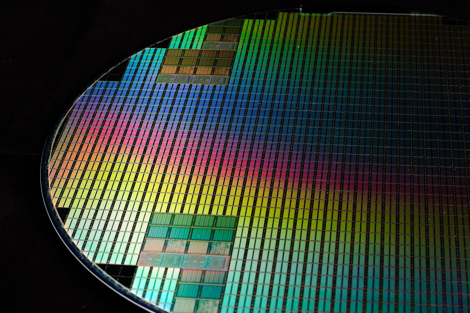
The eight-inch wafer, 200 millimeters across, is the workhorse of that segment. Samsung runs the lines at nodes from 180 nanometers down to 65, producing parts that do not need the density of a leading-edge processor and cannot absorb its price. The company began mass production at 180 nanometers in 2000, moved to 130 in 2002, to 90 in 2006 and to 70 in 2011.
The retreat has been staged for a year. In early 2026 Samsung decided to close only S7, one of three 8-inch fabs at its Giheung complex, by the end of this year, keeping S6 and S8 running. On the first-quarter earnings call in April, Kang Seok-chae, a vice president in the foundry business, said the lines serving power semiconductors, display driver chips and image sensors would be shut in sequence. The foundry stopped accepting new 8-inch orders this year.
The logic is arithmetic. Samsung’s foundry unit trails TSMC, which held 73% of the pure-play market in the second quarter, according to Counterpoint Research. Holding mature 200-millimeter capacity while paying for advanced nodes is a bill the company has decided not to carry. Workers and equipment move to 12-inch lines, where the customers with the largest budgets are.
The problem is that the capacity does not disappear into a market with room for it. DB HiTek and SK Keyfoundry, the two main Korean operators of 8-inch plants, are running near full. Industry forecasts put global 8-inch utilization around 90% this year, and DB HiTek has guided to 98%. “DB HiTek and SK Keyfoundry are also operating at full capacity, so we would have to look for overseas foundries to handle additional production,” an executive at a fabless customer told The Elec.
Taiwan has little spare 200-millimeter capacity, and TSMC has been trimming its own mature lines. China has capacity, but American and European customers have been pushing Chinese-made chips out of their bills of materials, which makes a transfer politically expensive even where it is technically simple.
Moving up to 12-inch is not a simple answer either. Products designed at 90 to 180 nanometers were built there for cost and for the physics: analog and power devices need specialized high-voltage processes that do not shrink cleanly. A redesign means new masks, new qualification, new customer audits, and a year or more before revenue.
Some buyers are already stockpiling wafers from Samsung while they can, which ties up capital in inventory and warehouse space and does not solve the eventual requalification. Others are asking Seoul to intervene. “Given that Samsung Electronics has provided four years of notice, it is difficult to characterize the decision as unilateral,” another industry official said. “However, domestic capacity is full, China is not an option, and foundries in Taiwan and the United States also have little spare capacity.”
Four years is a long time by the standards of a product cycle and short by the standards of a fab. Qualification at a new foundry often runs six months to a year for a mature analog part, longer if the customer sells into automotive. Read backwards from the end of 2030, the deadline for most of these companies is closer to 2027 than it looks.
The demand side argues against the exit. Eight-inch capacity is not being abandoned because nobody wants it. Power-management chips for AI servers, driver chips for larger displays and sensors for vehicles have all pulled on mature nodes, which is why the remaining plants can charge more. Samsung is leaving a business that is tightening because the returns on the business it is entering are larger.
That is the same calculation TSMC has made in slower steps, and the same one that has kept the smaller Korean foundries at full utilization. The difference is that Samsung’s customers have four years to find somewhere else, and the somewhere else is already booked.
For Samsung, the exit removes a distraction and a cost center at the moment its foundry business is trying to convince customers that it can be trusted with the most advanced work. Mature nodes carry low margins, long customer relationships and constant pressure from Chinese competitors adding capacity. Walking away from them frees engineers for the 2-nanometer fight, which is where the company’s capital and reputation are now committed.
Whether that trade works depends on a part of the business that does not appear in the announcement. A foundry’s customers judge it on whether the older lines keep running while the new ones ramp. Every fabless company that has to requalify a product somewhere else in the next four years will remember which supplier stopped answering.