The most valuable piece of silicon in an AI server is not the processor. It is the stack of memory chips mounted beside it, and the small wafer at the bottom of that stack is where the competition has moved.
Samsung Electronics plans to build that wafer, known as the base die, at its second fabrication plant in Taylor, Texas, according to Maeil Business Newspaper, which reported the plan on Nov. 2. The customers named in the report are AMD and Nvidia, the two largest suppliers of the accelerators that high-bandwidth memory plugs into. Capacity set aside for the work has already been committed, the newspaper said.
High-bandwidth memory is made by stacking layers of DRAM vertically and connecting them with thousands of microscopic channels that run through the silicon. The stack sits on a foundation wafer that carries the wiring out to the processor package. For the first two generations of the technology, that foundation was a simple buffer manufactured on a memory process, and it did little beyond routing signals.
That has changed as the stacks have grown taller and the interfaces between memory and processor have become the limiting factor. The bottom layer now holds logic: test circuits, power delivery, and in the more ambitious designs, functions that used to sit on the processor package. Making it requires a logic process, not a memory one, which is why memory makers have been buying capacity from foundries rather than building the wafers themselves.
That dependency is the opening Samsung is trying to exploit. It is the only one of the three large memory producers that also runs a foundry business at scale, and it has been trying to sell customers a package rather than a component: memory wafers, logic wafers and the advanced packaging that joins them, contracted together. For a customer designing an accelerator, dealing with one supplier for three parts of the bill of materials removes a set of handoffs that have become a scheduling problem.
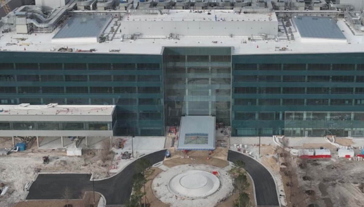
The Taylor site gives that pitch a geographic argument as well. Texas is where a large share of American chip design and server assembly sits, and a wafer finished in Taylor does not cross an ocean before it reaches a packaging line. The first plant at the site has been assigned advanced-node work for Tesla, with production targeted for 2027, according to the same report. The second plant is to break ground this year and is meant to reach volume manufacturing at 2 nanometers by 2030.
The timetable is the part that deserves scrutiny. A fab that starts construction this year and reaches 2-nanometer volume in 2030 is running a schedule that assumes no slips in tool installation, process qualification or customer tape-outs, and the industry’s record on all three is mixed. Samsung’s foundry business has spent years trying to close a yield gap with its larger rival, and every customer it wins is also a customer that will test whether the gap has closed.
Nvidia’s participation is the more consequential of the two names. The company buys memory from all three producers and has historically kept its suppliers in competition on price and on qualification. Placing base-die work with Samsung, if the report is accurate, would give Nvidia a second source for a part that has been concentrated, and would give Samsung a reference customer whose requirements set the standard for the rest of the market.
AMD’s interest is easier to explain. The company has been gaining share in accelerators by selling systems rather than chips, and it has less bargaining power with its memory suppliers than Nvidia does. A foundry that will take its base-die design and pair it with memory and packaging under one contract is worth more to AMD than a slightly better price on DRAM.
None of this is confirmed by the companies involved. Samsung has acknowledged the Taylor site and its broader foundry ambitions but has not named customers for the second plant. Nvidia and AMD do not comment on supplier arrangements. The report attributed its account to industry sources, and the details that matter most, which generation of memory the work covers and when the first wafers are due, were not disclosed.
Analysts said the strategic logic is sound regardless of the specific customers. The memory business has been cyclical for four decades because producers all sell a commodity that is priced by the market. A foundation wafer that carries a customer’s own logic, made on a foundry process and sold with packaging attached, is closer to a custom part, and custom parts are priced by negotiation rather than by the spot market.
The risk is that the custom part does not stay custom. If the foundation layer becomes standardized again, or if the processor makers decide to build it themselves, Samsung will have spent billions on capacity for a component that anyone can buy. That is the bet being placed in Taylor, and it will not be settled until the first stacks come off the line.