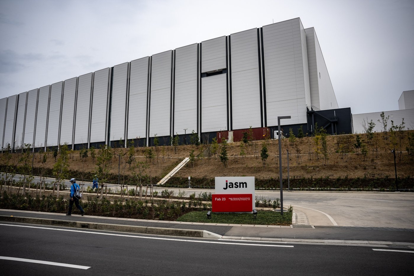
The approval that mattered arrived on October 16, from a ministry rather than a customer. Japan’s Ministry of Economy, Trade and Industry signed off on a revised plan for the second factory of JASM, the TSMC subsidiary in Kumamoto, allowing it to manufacture 3-nanometer logic instead of the 6- and 12-nanometer chips it was originally designed for. Japanese media reported the investment at more than $23 billion.
The number attached to the output is smaller than the headline. The first phase is certified at 6,000 wafers a month, a fraction of the 48,000 wafers of mature-node capacity in the design the ministry approved earlier. The gap between those two figures is the part of the story that will determine whether this is an industrial policy success or an expensive gesture.
A 3-nanometer wafer is not interchangeable with a 6-nanometer wafer. Each one carries far more transistors and, at TSMC’s pricing, several times the revenue. Six thousand wafers a month of leading-edge logic is a meaningful facility by the standards of specialty foundries and a modest one by the standards of TSMC’s Taiwan fabs, which run at multiples of that volume per site.
The constraint is lithography. Producing at this node requires extreme ultraviolet machines, and the supply of those tools is allocated years in advance and dominated by a single vendor. Every leading-edge fab under construction in Arizona, Dresden and Kumamoto is competing for the same delivery slots. Capacity at Kumamoto is therefore a function of how many scanners TSMC can route there, not of how much land it has cleared.
Money moved in the opposite direction from ambition. The subsidy cap for the project was set at 645.15 billion yen, below the 732 billion yen the government had earlier indicated, because the revised plan involves less total output than the original. The state is paying for capacity, and when capacity shrinks, so does the check. That is a more disciplined arrangement than the announcements of two years ago implied, and a less generous one.
What Japan gets for the money is a first. No other facility in the country can produce logic at this density, and the presence of the capability changes what Japanese companies can design domestically. Semiconductor equipment makers, materials suppliers and the packaging industry that surrounds Kumamoto all gain a customer with requirements that force them up the technology curve, which was the stated purpose of the subsidy program from the beginning.
The first Kumamoto fab is the argument for patience. It began volume production in late 2024 at 12- to 28-nanometer, is majority-owned by TSMC with Sony, Denso and Toyota holding minority stakes, and has run through the ordinary difficulties of a new site. A magnitude 7.1 earthquake on July 28 halted operations for equipment inspection, and production was restored over the following weeks. Building a fab in a new country is a decade-long project with bad quarters inside it.
TSMC’s own language has been careful. The company said through its Japan account on October 20 that production and investment will be implemented in phases according to market demand and government support, which is a commitment to the site and a hedge on the volume. A fab that starts at 6,000 wafers and expands later is cheaper to slow down than one built at full scale from the beginning.
That hedging is rational for a company that carries the capital cost of every leading-edge plant. TSMC is building simultaneously in Taiwan, Arizona, Germany and Japan, and each site needs the same scarce tools and the same small pool of experienced process engineers. Sequencing the expansions is how a company avoids owning four half-empty fabs when demand pauses, as it has paused before.
For Japan, the strategic value does not depend on the wafer count. The country has spent a decade trying to rebuild an industry it once led, and the policy has shifted from supporting domestic champions to inviting foreign ones with capital and customers attached. A 3-nanometer line, even a small one, puts Japanese suppliers inside the most demanding manufacturing process in the world, which is knowledge that does not leave when a subsidy expires.
For TSMC, the Kumamoto expansion is a hedge against geography. Taiwan produces the overwhelming majority of the world’s leading-edge logic, a concentration that customers and governments now treat as a risk to be priced. Building capacity in Japan, Arizona and Germany costs more per wafer and buys something the company cannot manufacture in Hsinchu: the political permission to keep selling.
The unresolved item is demand. The plant is scheduled to begin production in December 2028, by which point the current wave of AI spending will have either continued or corrected, and the customers who sign for its output will be making commitments in 2027. A 6,000-wafer line can be sold out years ahead if the cycle holds, and can sit underused if it does not.
Trade ministry approvals are not orders. What the October 16 decision establishes is that Japan will have the capability, that the government will pay a defined share of the cost, and that the volume will be small enough to expand or to leave alone. The rest depends on a market that has been enthusiastically wrong about timing before, and on a supply chain that will decide how many of those machines arrive.