
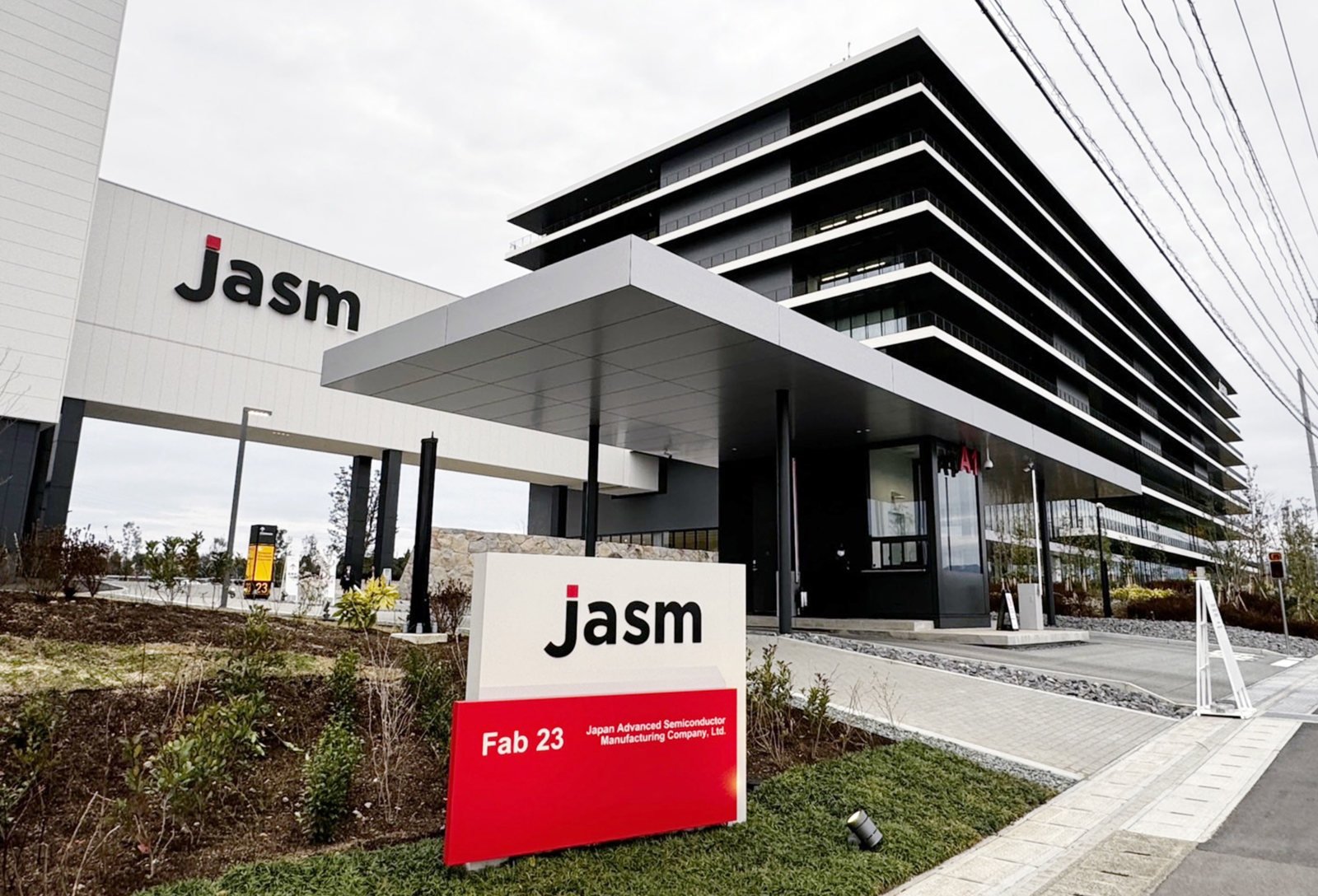
In Kikuyo, a town on the plain west of Kumamoto city, the second building on TSMC’s Japanese site has been rising next to the first for more than a year. Until this week, the plan for what goes inside it called for chips two generations behind the leading edge. That plan is gone.
Japan’s Ministry of Economy, Trade and Industry approved the change on October 16, allowing TSMC to dedicate the second fab to 3-nanometer production instead of the 6-nanometer and 12-nanometer process it had originally filed. It would be the first 3-nanometer plant in Japan.
The capacity figure tells the more interesting story. The revised plan calls for 6,000 wafers a month, against 48,000 in the original filing, and the final number depends on how large the subsidy turns out to be. Output is scheduled to begin in December 2028.
At roughly twenty thousand dollars a wafer, a figure in the range quoted for leading-edge 3-nanometer output, 6,000 wafers a month works out to about 1.4 billion dollars of annual revenue at full yield and full price. A single advanced fab of the kind TSMC operates in Taiwan runs at ten times that scale. This one is a foothold, not a factory.
Digitimes reported that the Japanese subsidy is capped at about 4.1 billion dollars, that the ministry has already begun requesting funds in the next fiscal year’s budget, and that total assistance including the first fab is expected to exceed one trillion yen. Equipment spending across the two plants is expected to top 23 billion dollars.
Those numbers explain the arithmetic that both sides accepted. A 6,000-wafer line is too small to earn a return on the capital required for a leading-edge cleanroom. It is large enough to give Japan a working 3-nanometer process, a set of trained engineers and a reason for tool suppliers and materials companies to locate nearby. The subsidy is paying for the option, not for the output.
The first fab, a joint venture with Sony, Denso and Toyota in which TSMC holds a majority, opened in early 2024 and makes 12-nanometer, 16-nanometer, 22-nanometer and 28-nanometer chips for automotive and industrial customers. Those are the parts Japanese manufacturers buy in volume, and the plant was sized for them.
The second fab was always the strategic one. Japan’s government has been trying to rebuild a semiconductor industry it lost to Taiwan and Korea over two decades, and it has pursued two paths at once: attracting a foreign leader to build a plant that employs Japanese workers and suppliers, and funding Rapidus, a domestic venture trying to reach 2-nanometer production in Hokkaido by 2027.
The two paths compete for the same scarce resources. Advanced fabs need process engineers, and Japan has fewer of them than the plants now under construction will require. They also need water. Kumamoto’s groundwater has supported agriculture in the region for centuries, and the first fab’s wells were negotiated with local authorities before construction began.
Delay is built into the schedule. A 3-nanometer plant that starts output in December 2028 will be entering a market where 2-nanometer volume production has been running for two years and where TSMC’s A16 process, with a new power delivery scheme, is expected in the same window. The node will be mature by the time the wafers come out, which is fine for customers who need a proven process and less fine for a government that wanted the frontier.
Automotive customers are the likely anchor. Chips for advanced driver assistance, vehicle control and infotainment have moved toward 5-nanometer and 3-nanometer designs, and Japanese carmakers have been buying those parts from Taiwan and Korea. A domestic line shortens the supply chain that broke in 2021, when a fire at a single plant idled assembly lines worldwide.
The economics of a small line work differently from those of a large one. Fixed costs per wafer rise when volume falls, and yield learning takes longer on a line that runs few lots. TSMC can absorb that because the plant is a fraction of its total capacity and because the subsidy covers a large share of the capital. A pure commercial operator would not build it.
The company’s broader expansion follows the same logic of dispersion. It is building 2-nanometer capacity in Arizona, where the first phase has been slower and more expensive than the Taiwan equivalent, and it has committed to keeping its most advanced process in Taiwan for the initial ramp. Each overseas site is justified partly by customer demand and partly by the governments that want the capacity inside their borders.
For Japan, the approval is a win with a caveat attached. The country gets a 3-nanometer process, the training that comes with it, and a claim on the supply chain for the chips that will sit in its cars and its data centers. It does not get volume, and volume is what determines whether an industry sustains itself.
For TSMC, the calculation is about relationships. Japanese customers, Japanese tools and Japanese materials are part of a supply chain the company depends on, and a small leading-edge line is a modest price for keeping those ties strong while a competitor courts the same partners.
What happens next is a budget negotiation. The 6,000-wafer figure is contingent on the subsidy, and the ministry’s request will be weighed against other claims in a year when the government is also funding Rapidus and a domestic advanced packaging effort. If the money is trimmed, the wafer count falls with it.
Analysts said the number to watch is not the node but the ramp: whether the plant reaches volume on schedule, and whether the suppliers that follow it to Kumamoto build plants of their own. A single small fab can be a subsidy project. A cluster of them is an industry, and the difference shows up in the second wave of investment rather than the first.